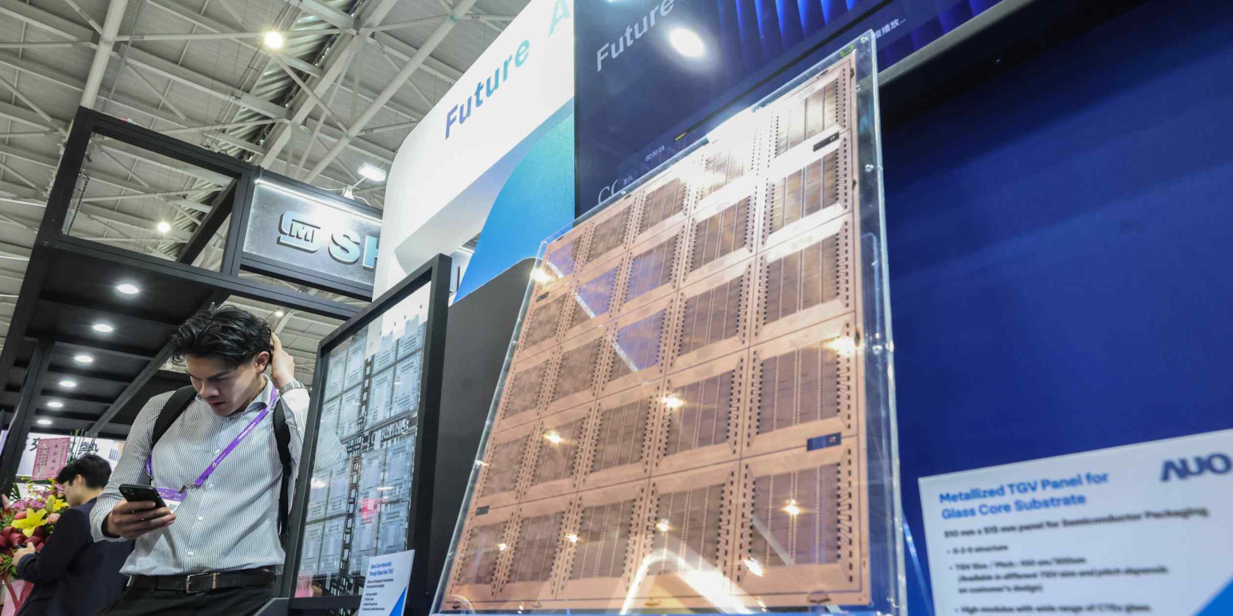
东京 -- 台湾一家主要的面板制造商 AUO 在 9 月初举行的台湨半导体展览会 Semicon Taiwan 上展出了一块玻璃基半导体衬底,引起了广泛关注。
TOKYO -- AUO, a major Taiwanese maker of display panels, drew attention when it showcased a glass-core substrate for semiconductors at Semicon Taiwan, an international trade show held in early September.
这块边长略大于 50 厘米的平方衬底由 AUO 和美国玻璃制造商 Corning 共同开发并展出。AUO 在 Corning 加工处理的玻璃材料上形成了布线层及其他组件。
The square substrate, measuring slightly more than 50 centimeters on each side, was developed and exhibited by AUO and U.S. glassmaker Corning. AUO formed wiring layers and other components on glass material processed by Corning.
玻璃正成为下一代半导体衬底的主要候选材料,传统上这些衬底多使用树脂和其他有机材料,而台湾公司正准备进行开发和大规模生产。这种转变的推动力在于日益强大的人工智能芯片需求。
Glass is emerging as a leading candidate for next-generation semiconductor substrates, which traditionally have used resin and other organic materials, and Taiwanese companies are preparing for development and mass production. The shift is driven by the need to accommodate increasingly powerful artificial intelligence chips.
用于人工智能的半导体将计算芯片和高速内存封装在一起,因此需要更大的衬底。树脂衬底在受热时容易膨胀和收缩,且随着尺寸增大,变形问题愈发突出。玻璃抗变形性能出色,非常适合制造更大、更密集集成的衬底。
Semiconductors used for AI pack together computing chips and high-speed memory, meaning larger substrates are needed. Resin substrates expand and contract relatively easily when exposed to heat, and warping becomes a problem as they grow larger. Glass resists warping, making it well suited for larger, more densely integrated substrates.
今年 5 月在美国佛罗里达州举行的一次国际半导体会议上也出现了类似的动向。英特尔透露,该公司利用现有常规树脂衬底的生产线,成功制造出了带有堆叠布线层的玻璃基原型衬底。
Similar moves were seen at an international semiconductor conference in the U.S. state of Florida in May. Intel disclosed that it had produced a prototype glass-core substrate with stacked wiring layers using an existing production line for conventional resin substrates.
英特尔多年来一直在研发玻璃基衬底。该公司表示,其原型衬底实现了“No SeWaRe”,即衬底上没有微裂纹。这一突破被英特尔视为将该技术商业化的重要一步。
Intel has been developing glass-core substrates for years. The company said it achieved "No SeWaRe" with its prototype, meaning no micro-cracks on the substrate. The company considers the development an important step toward commercialization of the technology.
自2023年分享这张玻璃芯基片产品的照片以来,英特尔一直在继续与玻璃芯基片合作。(英特尔)但挑战仍然存在,包括验证玻璃芯基片的可靠性和克服大规模生产的困难。因此,由树脂等材料制成的有机核心目前可能仍将是主流。但台湾公司正在积极推进玻璃技术的商业化。
Intel has continued to work with glass-core substrates since sharing this photograph of one such product in 2023. (Intel) But challenges remain, including verifying the reliability of glass-core substrates and overcoming the difficulties of mass production. Organic cores made from materials such as resin therefore likely will remain mainstream for now. But Taiwanese companies are moving aggressively toward commercialization of the glass technology.
7月底,友达光电表示,将把部分资本支出转向玻璃芯基片的试点生产线。董事长兼首席执行官彭双朗表示,该技术需要两到三年的时间才能成熟,但表示对其前景充满信心,并指出该公司与玻璃的合作已有近30年。
At the end of July, AUO said it would redirect part of its capital spending toward a pilot production line for glass-core substrates. Chairman and CEO Peng Shuang-Lang said it would take two to three years for the technology to mature, but expressed confidence in its prospects, noting that the company had been working with glass for nearly 30 years.
台湾另一家主要面板制造商群创集团也将玻璃芯基片视为关键战略领域,并表示正在继续与海外合作伙伴合作开发。该公司的目标是应用其为电视和个人电脑开发的面板制造专业知识来创建新的半导体业务。
Innolux, another major Taiwanese panel maker, also sees glass-core substrates as a key strategic field and says it is continuing development with overseas partners. The company aims to apply the panel manufacturing expertise it developed for televisions and personal computers to create a new semiconductor business.
玻璃导电性较差。为了将其用作基片,制造商需要“玻璃通孔”或TGV技术,其中在基片中形成微小孔,并填充金属以电连接其两侧。设备制造商正在开发该过程的机械和其他系统。
Glass conducts electricity poorly. To use it as a substrate, manufacturers need "through glass via," or TGV, technology, in which microscopic holes are formed in the substrate and filled with metal to electrically connect its two sides. Equipment makers are developing machinery and other systems for the process.
半导体检测设备制造商Spirox首席执行官Paul Yang表示:“TGV正在逐步从技术开发和中试生产转向大批量制造。”
"TGV is gradually moving from technology development and pilot production toward high-volume manufacturing," said Paul Yang, CEO of semiconductor inspection equipment maker Spirox.
生产TGV加工设备的E & R Engineering表示,与基片制造商对其机械的验证已进入最后阶段。7月,该公司指出,有迹象表明,2027年下半年将出现对设备的具体需求,早于研究公司和其他公司的预期。
E&R Engineering, which makes TGV processing equipment, said verification of its machinery with substrate manufacturers has entered its final stages. In July, the company noted signs that concrete demand for equipment would emerge in the second half of 2027, earlier than research companies and others had expected.
日本的供应商们也在致力于研发玻璃材料与半导体基板。住友化学于7月份宣布,已与三星电机达成协议,将共同组建一家从事玻璃芯材业务的合资企业,目标是在2027年下半年建立起大规模生产体系。大日本印刷则于去年启用了自己的试验生产线。
Japanese suppliers also are working on glass materials and semiconductor substrates. Sumitomo Chemical said in July that it had agreed with Samsung Electro-Mechanics to form a joint venture in the glass-core business, aiming to establish a mass production system in the second half of 2027. Dai Nippon Printing launched its own pilot line last year.
“为跟上人工智能技术的发展步伐,半导体的性能必须实现大幅提升,”一位在台湾半导体展上参展的日本材料制造商高管说道,“用于半导体研发与制造的材料同样需要取得显著进步。”
"To keep pace with advances in AI, semiconductors need a very significant leap in performance," said an executive at a Japanese materials maker exhibiting at Semicon Taiwan. "The same is true of the materials needed to develop and manufacture them."