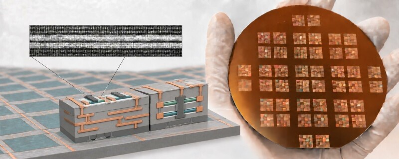
研究人员展示了一种控制二维半导体晶体生长起始位置的方法,这有望解决大规模制造下一代芯片时面临的一个障碍。该研究发表在《自然》杂志上,论文题为《通过蚀刻通量实现二维半导体的空间确定性核生成》,由包括韩国科学技术院(KAIST)和韩国初创公司TDS Innovation研究人员在内的团队撰写,并于10月7日发表。
Researchers have demonstrated a way to control where 2D semiconductor crystals begin growing, potentially addressing an obstacle to manufacturing next-generation chips at scale, according to a study published in Nature. The paper, "Spatially deterministic nucleation of 2D semiconductors by etching flux," was authored by a team including researchers at KAIST and South Korean startup TDS Innovation and published on October 7.
该技术利用蚀刻通量在每个图案化生长区域内除几何中心外的所有位置抑制新晶体的形成。二维材料在原子层面极薄,而非字面意义上的二维。石墨烯或许是最著名的例子,它是由单层碳原子组成,但由于缺乏内在带隙,不适用于传统开关晶体管。某些过渡金属二硫化物(TMDs)的单层,如二硫化钼(MoS₂),具有带隙,正被研究作为未来晶体管和其他纳米器件的材料。
The technique uses an etching flux to suppress the formation of new crystals everywhere within each patterned growth region except at its geometric center. Two-dimensional materials are atomically thin rather than literally two-dimensional. Graphene, perhaps the best-known example, is a single layer of carbon atoms, but its lack of an intrinsic band gap makes it unsuitable for conventional switching transistors. Monolayers of some transition-metal dichalcogenides (TMDs), such as molybdenum disulfide (MoS₂), do have a band gap and are being investigated as materials for future transistors and other nanoscale devices.
然而,当在晶圆上生长时,二维半导体晶体通常会在随机点开始形成,或者说“核生成事件在生长区域内的随机位置以随机方式发生”,正如论文所述。这意味着多个晶体会形成,随着它们的生长和汇合,它们之间会形成边界,这些边界会降低电气性能并使器件性能不均匀。为了在每个图案化区域内促进单个晶体的形成,研究人员开发了一种他们称为蚀刻通量介导的单中心核生成(EF-SCN)过程。
When grown on a wafer, however, 2D semiconductor crystals typically start forming at random points, or "nucleation events occur stochastically at random sites within the growth region," as the paper puts it. This means that multiple crystals form, and as they grow and meet, they create boundaries between them that degrade electrical performance and make devices less uniform. To encourage a single crystal to form in each patterned region, the researchers developed what they call an etching-flux-mediated single-centred nucleation (EF-SCN) process.
氧化物屏障释放的氧气产生横向蚀刻通量,除了图案的几何中心外,该通量会抑制核生成。研究人员利用这一过程制造了可工作的场效应晶体管(FETs),这是现代芯片的基本构建块。
Oxygen released from an oxide barrier creates a lateral etching flux that suppresses nucleation except at the pattern's geometric center. The researchers used the process to build working field-effect transistors (FETs), the basic building blocks of modern chips.
他们报告了更高的载流子迁移率——这是衡量电荷在材料中移动容易程度的指标——高于之前报道的选择性生长MoS₂晶体管的水平。在对两厘米基板的单独测试中,该工艺在400个图案化位点中产生了397个单晶——良率达99.3%。这对于规模化具有前景,尽管尚未演示商用芯片生产。论文共同作者Kibum Kang是TDS Innovation的联合首席执行官,该公司开发用于二维半导体器件的设备和材料。
They reported higher charge-carrier mobility – a measure of how readily charge moves through the material – than previously reported for selectively grown MoS₂ transistors. In a separate test across a two-centimeter substrate, the process produced single crystals at 397 of 400 patterned sites – a yield of 99.3 percent. That is promising for scaling up, although it is not yet a demonstration of commercial chip production. Paper co-author Kibum Kang is co-CEO of TDS Innovation, which develops equipment and materials for 2D semiconductor devices.
该公司表示,将二维半导体器件堆叠在硅芯片上,可以使逻辑和存储更接近,在给定面积内实现更多功能,并减少在它们之间传输数据所花费的时间和能源。二维半导体材料也正在被研究用于CFETs(互补型场效应晶体管),这种晶体管将n型和p型晶体管垂直堆叠,而不是并排放置。这种3D堆叠方式已被IBM和英特尔展示。
The firm says stacking 2D semiconductor devices on silicon chips could bring logic and memory closer together, fitting more functions into a given area and reducing the time and energy spent moving data between them. Two-dimensional semiconductor materials are also being investigated for CFETs (complementary field-effect transistors), which stack n-type and p-type transistors vertically rather than placing them side by side. This kind of 3D stacking has been shown off by IBM and Intel.
Kang表示:“基于我们能够控制晶体生长起始位置的能力,我们将在需要的地方均匀形成高质量的二维单晶,并将其发展为一种下一代半导体工艺,使逻辑和存储更接近。”论文未说明何时能看到以这种方式制造的二维半导体用于生产芯片,TDS的Jony Jung告诉我们:“我们的目标是实现二维半导体在2030年左右的商用应用。我们认为,包括物理AI和机器人在内的AI需求加速增长可能有助于推动其应用提前,尽管生产时间表将取决于进一步的验证。”®
"Building on this ability to control where crystal growth begins, we will form high-quality 2D single crystals uniformly where we want them and develop it into a next-generation semiconductor process that brings logic and memory closer together," Kang states. The paper doesn't say when we can expect to see 2D semiconductors made this way in production chips, TDS's Jony Jung told us: "We are aiming to enable commercial use of 2D semiconductors around 2030. We believe accelerating demand from AI, including physical AI and robotics, could help bring adoption forward, although production timing will depend on further validation." ®