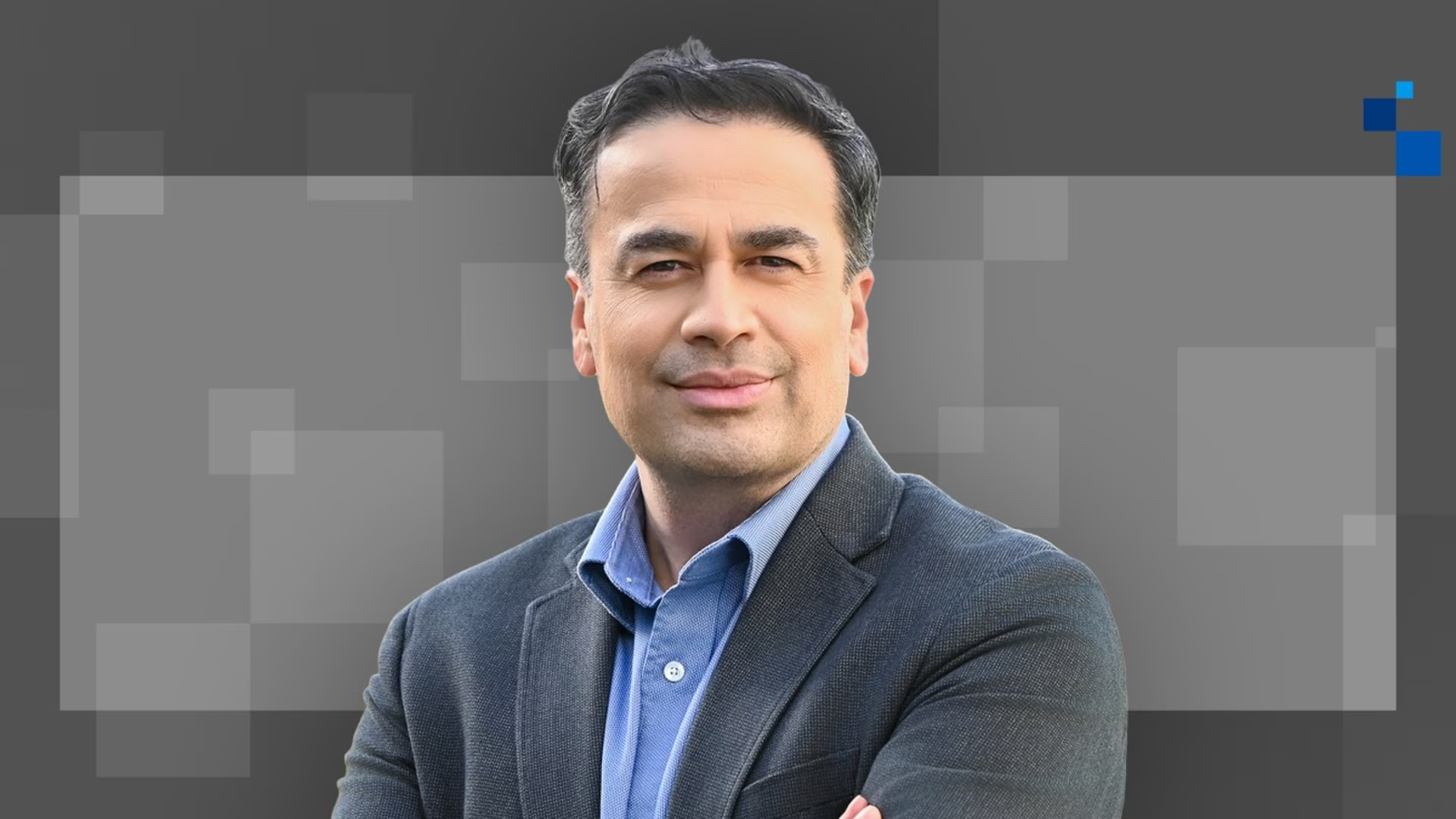
英特尔首席技术官普什卡尔·拉纳德表示,即使英特尔想要,也无法将尖端晶圆产量提高10倍。世界缺乏芯片制造工具。他告诉德瓦克什·帕特尔,在《德瓦克什播客》节目中,产量翻倍大约是极限。帕特尔在对英特尔位于俄勒冈州最先进晶圆厂进行为期两天的参观期间录制了这一期节目。
Intel could not make 10 times more leading-edge wafers even if it wanted to, says its chief technology officer, Pushkar Ranade. The world lacks the chipmaking tools. Doubling output is about the limit, he told Dwarkesh Patel on the Dwarkesh Podcast. Patel filmed the episode during a two-day tour of Intel’s most advanced fab in Oregon.
帕特尔询问世界是否拥有足够的工具,让英特尔生产出10倍数量的尖端晶圆。拉纳德说:“不是10倍,但大概2倍,是的。”
Patel asked whether the world had enough tools for Intel to make 10 times as many leading-edge wafers. “Not 10X, but probably 2X, yes,” Ranade said.
帕特尔指出,十年来AI算力每年大约增长三倍。拉纳德表示,只有当每个供应商的产出也同步加快时,产量才能更快增长。
Patel noted that AI compute has grown about threefold a year for a decade. Ranade said output could only rise faster if every supplier did too.
他说:“除非每个人都生产更多,否则你无法增加产出。”他点名了设备供应商、他们的供应商以及分级供应商。
“Unless everybody produces more, you can’t increase the output,” he said, naming equipment suppliers, their suppliers and their sub-suppliers. Tools are the bottleneck ASML makes fewer than 100 EUV lithography machines a year, Patel said.
帕特尔说,阿斯麦每年生产的极紫外光刻机不足100台。英特尔、台积电和存储芯片制造商都在争夺它们。拉纳德表示,极紫外光刻是最大的瓶颈,但不是唯一的瓶颈,因为大多数芯片制造设备都供不应求。一旦像18A这样的工艺确定下来,英特尔就需要它所设计使用的那些确切工具。他说,英特尔可以为下一代节点14A重复使用约80%的18A工具。
Intel, TSMC and the memory makers all compete for them. Ranade said EUV is the biggest bottleneck but not the only one, as most chipmaking equipment is in short supply. Once a process like 18A is set, Intel needs the exact tools it was designed for. Intel can reuse about 80% of the 18A tools for the next node, 14A, he said. Tools ordered today take about 18 months to arrive, Ranade said, which takes buyers into 2028.
拉纳德说,今天订购的工具大约需要18个月才能到货,这将买家带入2028年。在此基础上新建一座晶圆厂,意味着要等到本十年末。他补充说,如果一年前英特尔知道现在知道的情况,本会在设备上投入更多资金。拉纳德说:“基于我们现在所知,我认为我们会投入更多。”“我们已经做到了”在谈到台积电时,拉纳德在规模和技术之间划清了界限。他说,台积电出货的晶圆多得多,在这方面追赶将是渐进的。
Building a new fab on top of that means the end of the decade. He added that Intel would have spent more on equipment had it known a year ago what it knows now. “Knowing what we know now, I think we’ll be investing more,” Ranade said. “We’re already there”On TSMC, Ranade drew a line between scale and technology. TSMC ships far more wafers, and catching up on that will be gradual, he said.
拉纳德说:“如果你指的是仅在技术层面追赶,我认为我们已经做到了。”
“If you meant catching up in terms of just the technology, I think we’re already there,” Ranade said.
Patel 引用 SemiAnalysis 的数据指出,Intel 预计 2028 年推出的 14A 工艺在晶体管密度上将与 TSMC 的 N2 工艺持平。“我对你的基准测试持不同意见,”Ranade 回应道,并补充说密度只是衡量标准之一。
Patel cited SemiAnalysis figures suggesting Intel’s 14A, due in 2028, would match TSMC’s N2 on transistor density. “I would dispute your benchmarking,” Ranade replied, adding that density is only one measure.
Chris Auth 负责 Intel 的制程开发。他表示,Intel 在 14A 上采用 ASML 的 High-NA EUV(高数值孔径极紫外光刻)设备,是因为其芯片将电源线移到了晶圆背面。TSMC 曾表示,这些设备对其而言目前尚不具备经济意义。Auth 认为这是因为 TSMC 缺乏背面供电技术。TSMC 已宣布将在其 A16 节点推出自家版本,称为 Super Power Rail。
Chris Auth leads Intel’s process development. He said Intel offers ASML’s High-NA EUV machines on 14A because its chips move power lines to the back of the wafer. TSMC has said the machines do not make economic sense for it yet. Auth put that down to TSMC lacking backside power. TSMC has announced its own version, called Super Power Rail, for its A16 node.
Auth 还透露,18A “最初没有 PDK”。PDK 是外部客户在代工厂制造芯片所需的设计工具包。他表示,14A 从一开始就会提供 PDK。
Auth also said 18A “started out not having a PDK”. That is the design kit outside customers need to build chips at a foundry. He said 14A will have one from the start.
内存、Musk 与洁净室 Ranade 对 Intel 退出内存业务坦言相告。Intel 几年前将其闪存业务出售给了 SK Hynix。
Memory, Musk and clean rooms Ranade was frank about Intel’s exit from memory. Intel sold its flash business to SK Hynix a few years ago.
“显然,事后看来,出售闪存业务的时机可能并不明智,”Ranade 说。他补充称,目前内存的供应短缺比计算芯片更为严重。
“Clearly, in hindsight, probably not the smartest time to sell off a flash memory business,” Ranade said. He added that the supply crunch is worse for memory than for compute today.
Intel 还在与 Elon Musk 合作 Terafab,这是 Tesla 和 SpaceX 计划在得克萨斯州建设的芯片工厂。Intel 首席执行官本月早些时候告诉彭博社,Intel 将继续参与该项目。TSMC 表示,如果由其运营晶圆厂,愿意参与 Terafab 合作。Ranade 说,建厂比造车复杂得多,因此 Intel 提议与 Musk 合作以加快其建厂进程。
Intel is also working with Elon Musk on Terafab, the chip plant Tesla and SpaceX plan in Texas. Intel’s chief executive told Bloomberg this month that Intel will stay on the project. TSMC has said it is open to working on Terafab if it runs the fab. Ranade said building a fab is far more intricate than building a car, so Intel offered to work with Musk to speed his up.
他还质疑了行业一些最根深蒂固的习惯,包括洁净室。“今天真的还需要洁净室吗?”他问道。他说,现有厂商不会冒险在量产线上测试这一点。一座新厂可以从白板起步。节目播出后,Ranade 在 X 上感谢 Patel。
He also questioned some of the industry’s oldest habits, including the clean room. “Do you really need a clean room today?” he asked. No incumbent would risk testing that on a live line, he said. A new fab can start from a clean slate. Ranade thanked Patel on X after the episode aired.
@dwarkesh_sp 很高兴与你合作并接待你来到我们的俄勒冈园区!喜欢你把那些广泛而漫长的对话浓缩成简练连贯的内容!2026 年 10 月 22 日
@dwarkesh_sp It was fun to work with you and host you at our Oregon campus! Love how you put all the many hours of wide-ranging conversations together in a succinct and coherent way! October 22, 2026