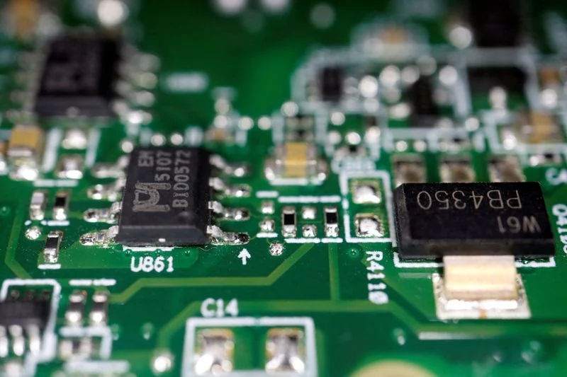
台北,11月6日电 —— 全球建设人工智能基础设施的竞赛正在释放数十亿美元的投资,涌向先进芯片封装领域。这一曾经不起眼的技术环节,已成为生产全球最强大处理器的关键瓶颹。
TAIPEI, Nov 6 - A global race to build AI infrastructure is unleashing billions of dollars of investment in advanced chip packaging, a once unglamorous aspect of technology that has become a critical bottleneck in turning out the world’s most powerful processors. As demand for artificial intelligence chips outstrips available packaging capacity, companies from Nvidia and AMD to lesser-known players in Taiwan are expanding production, while equipment makers develop new tools, interviews with more than a dozen industry executives and analysts show.
随着对人工智能芯片的需求超过现有的封装产能,从英伟达、超威半导体到台湾一些鲜为人知的厂商,都在扩大生产,同时设备制造商正在开发新工具,这是根据对十多位行业高管和分析师的采访得出的结论。
"Packaging was always that thing that you just didn’t worry about," former Intel chief executive Pat Gelsinger, now a partner at Playground Global, told reporters in Taipei recently.
“封装一直是你根本不用操心的事,”英特尔前首席执行官帕特·基辛格近日在台北对记者表示,他现为Playground Global合伙人。
Advanced packaging could eventually account for as much as half the value of a chip product, Gelsinger estimated, as some of today’s graphics and central processing units can integrate 10 or more chips, sometimes as many as 20.
基辛格估计,先进封装最终可能占芯片产品价值的一半,因为当今一些图形和中央处理单元可整合10颗甚至多达20颗芯片。
Revenue from advanced packaging is forecast to overtake that earned via the traditional route for the first time in 2026, says research firm Yole Group, with capital spending on the technology expected to near $28 billion.
研究机构Yole Group表示,先进封装的营收预计将在2026年首次超过传统封装路线,该技术的资本支出预计将接近280亿美元。
TAIWAN FIRM DOMINATES CHIP-ON-WAFER SUBSTRATE The world’s largest contract chipmaker, Taiwan’s TSMC, dominates the most sophisticated advanced packaging technology, including chip-on-wafer-on-substrate, or CoWoS.
台湾厂商主导晶圆上芯片基板封装 全球最大晶圆代工厂、台湾的台积电,主导着最尖端的先进封装技术,包括晶圆上芯片基板封装,即CoWoS。
The technology links separate pieces of silicon, such as processors and memory chips, on a shared base, to let them work together at high speed.
该技术将处理器和存储芯片等独立的硅片,在共享基板上连接起来,使它们能以高速协同工作。
It is widely used by Nvidia, AMD and Broadcom, as well as cloud companies developing their own AI chips.
英伟达、超威半导体、博通以及开发自家人工智能芯片的云端公司,广泛采用这项技术。但台积电的产能限制,促使一些芯片设计商寻求额外供应。
But TSMC’s capacity limits have spurred some chip designers to seek additional supply. Nvidia, for example, is providing billions of dollars in financing to expand CoWoS packaging capacity at Siliconware Precision Industries, or SPIL, a unit of Taiwan’s ASE Technology, said an industry executive familiar with the matter, who sought anonymity for lack of authorisation to talk to media.
例如,英伟达正在向台湾ASE科技旗下的硅统精密工业(SPIL)提供数十亿美元融资,以扩大其CoWoS封装产能,一位知情行业高管表示。该高管因未获授权与媒体交谈,要求匿名。
The funding will support new factory space and equipment, the executive said. The scale of the support has not previously been reported.
该高管表示,这笔资金将用于支持新的厂房和设备。此前从未有报道披露该支持的规模。
Nvidia did not respond to a request for comment. ASE said it does not comment on market rumours involving its customers.
英伟达未回应置评请求。ASE表示,不对涉及其客户的市场传闻发表评论。
A FUNDAMENTAL CHIPMAKING SHIFT The scramble to invest reflects a broader change in manufacturing of powerful chips, as more chip designers use advanced packaging to integrate multiple chips, such as processors and memory, into a single package. That allows the ensemble to work together faster as one system, in contrast with the practice of decades, when packaging served mainly to protect chips and provide the electrical connections to attach them to circuit boards.
芯片制造的根本性转变 投资热潮反映出强大芯片制造的更广泛变化,越来越多的芯片设计商采用先进封装,将处理器和内存等多颗芯片集成在一个封装中。
The shift comes as it become harder and costlier to win performance gains by shrinking and adding transistors, the tiny switches inside a chip.
这使得整体能够作为一个系统协同工作,速度更快,这与数十年来的做法形成对比,当时封装主要用于保护芯片,并提供将芯片连接到电路板的电气连接。
The newer packaging technique is especially important for AI chips, which need to shuffle vast amounts of data between processors and nearby memory.
这一转变发生在通过缩小和增加芯片内部的微小开关——晶体管来提升性能变得更加困难和昂贵的背景下。
Speeding up such transfers hastens the process of training and running AI models.
较新的封装技术对人工智能芯片尤其重要,因为这类芯片需要在处理器和附近内存之间传输海量数据。加快此类传输可加速人工智能模型的训练和运行过程。
A RACE FOR TSMC ALTERNATIVES TSMC’s tight capacity offers an opportunity for smaller suppliers, such as Taiwan’s Powertech Technology. "Everyone is looking for a solution outside TSMC," its chairman, D K Tsai, told reporters in August.
寻找台积电替代方案的竞赛 台积电产能紧张为较小的供应商提供了机会,例如台湾的力成科技。
"They don’t want to rely entirely on TSMC."
“每个人都在寻找台积电之外的解决方案,”力成科技董事长蔡丁来八月对记者表示,“他们不想完全依赖台积电。”力成科技(又称PTI)正押注于面板级封装,该技术使用较大的矩形面板,而非圆形晶圆,作为芯片封装平台。
Powertech, also known as PTI, is betting on panel-level packaging, which uses larger rectangular panels instead of round wafers as the chip packaging platform. This way, it can accommodate more chips in each production run and waste less material, an advantage as AI processors become larger and more complex.
这样,它可以在每次生产中容纳更多芯片,并减少材料浪费,随着 AI 处理器变得更大、更复杂,这一优势将更加明显。
PTI is working with AMD and Broadcom on the technology as the industry seeks to demonstrate its viability for larger, more complex chip packages used in AI and high-performance computing.

随着行业寻求证明该技术在 AI 和高性能计算中用于更大、更复杂芯片封装的可行性,PTI 正与 AMD 和 Broadcom 合作开发该技术。
"The most important thing right now is capacity," said PTI Senior Vice President Jim Lin, adding that customers were waiting for the company to ramp up production.
“目前最重要的是产能,”PTI 高级副总裁 Jim Lin 表示,并补充说,客户正等待该公司提升产能。
Powertech plans to invest $400 million in an advanced packaging joint venture with Broadcom in Singapore.
Powertech 计划在新加坡与 Broadcom 合资投资 4 亿美元用于先进封装。Tsai 表示,生产可能于 2028 年开始。
Production could begin in 2028, Tsai said. To support larger and more complex chip packages, TSMC is developing its own panel-based technology, called chip-on-panel-on-substrate, or CoPoS.
为支持更大、更复杂的芯片封装,TSMC 正在开发其自身的基于面板的技术,称为芯片-面板-基板(CoPoS)。
In April, it said it had built a pilot line and expected production to begin within a couple of years, but CoWoS remains TSMC’s main AI-packaging technology.
4 月,该公司表示已建成一条试产线,并预计生产将在几年内开始,但 CoWoS 仍然是 TSMC 的主要 AI 封装技术。
AMD has also unveiled investments of more than $10 billion across Taiwan’s semiconductor industry, including partnerships with ASE, SPIL and Powertech on advanced packaging.
AMD 还宣布在台湾半导体行业投资超过 100 亿美元,包括与 ASE、SPIL 和 Powertech 在先进封装方面的合作。
Asked if Powertech’s panel-level packaging technology could offer an alternative to TSMC’s technology, AMD Chief Executive Lisa Su did not directly address the question but acknowledged the need for more advanced packaging capacity.
当被问及 Powertech 的面板级封装技术是否可以作为 TSMC 技术的替代方案时,AMD 首席执行官 Lisa Su 没有直接回答这个问题,但承认需要更多先进封装产能。
"I think CoWoS and advanced packaging are super important for our high-performance computing going forward," Su told Reuters in Taipei in October.
“我认为 CoWoS 和先进封装对我们未来的高性能计算至关重要,”Su 在 10 月于台北接受路透社采访时表示。
"TSMC has been an incredible partner in advanced packaging, and we’re going to continue to do more together.
“TSMC 在先进封装方面一直是一家不可思议的合作伙伴,我们将继续一起做更多事情。是的,我们总体上确实需要更多产能。”微软 Azure 硬件负责人 Rani Borkar 表示,面板级封装在封装更大的 AI 芯片时可以减少材料浪费,尽管该公司尚未决定是否以及何时采用该技术。
And yes, we do need more capacity overall." Panel-level packaging would reduce material waste when packaging larger AI chips, said Microsoft Azure hardware chief Rani Borkar, though the company has not decided whether or when it will adopt the technology.
芯片设备制造商加入竞逐 包装热潮也为半导体设备制造商开辟了新市场。
CHIP EQUIPMENT MAKERS JOIN THE RUSH The packaging boom is also opening a new market for makers of semiconductor equipment.
此类公司传统上专注于芯片制造的早期阶段,当时电路被构建在硅片上。先进封装则在后期进行,当时芯片、内存或其他组件被组装成一个完成的高性能单元。
Such companies have traditionally focused on earlier stages of chipmaking, when circuitry is built onto silicon. Advanced packaging comes later, when chips, memory or other components are joined into a finished high-performance unit.
东京电子台湾总裁中岛正司表示,先进封装的增长速度远快于芯片制造设备市场,尽管其规模仍较小。
Advanced packaging was growing much faster than the market for chip-making gear, though it remained smaller, said Seiji Nakama, president of Tokyo Electron Taiwan.
美国设备商应用材料的一位官员表示,包括面板级技术在内的先进封装市场,可能在三到五年内显著增长。
The market for advanced packaging, including panel-level technology, could grow significantly within three to five years, said an official of US equipment maker Applied Materials.
“这是近期的事,”该公司副总裁斯里·凯萨普拉加达表示,该公司越来越专注于这种新形式。“不是像十年、十五年那么遥远。”
"It’s near-term," said Sree Kesapragada, a vice president at the company, which is increasingly focusing on the new format. "It’s not like, 10 years, 15 years off."