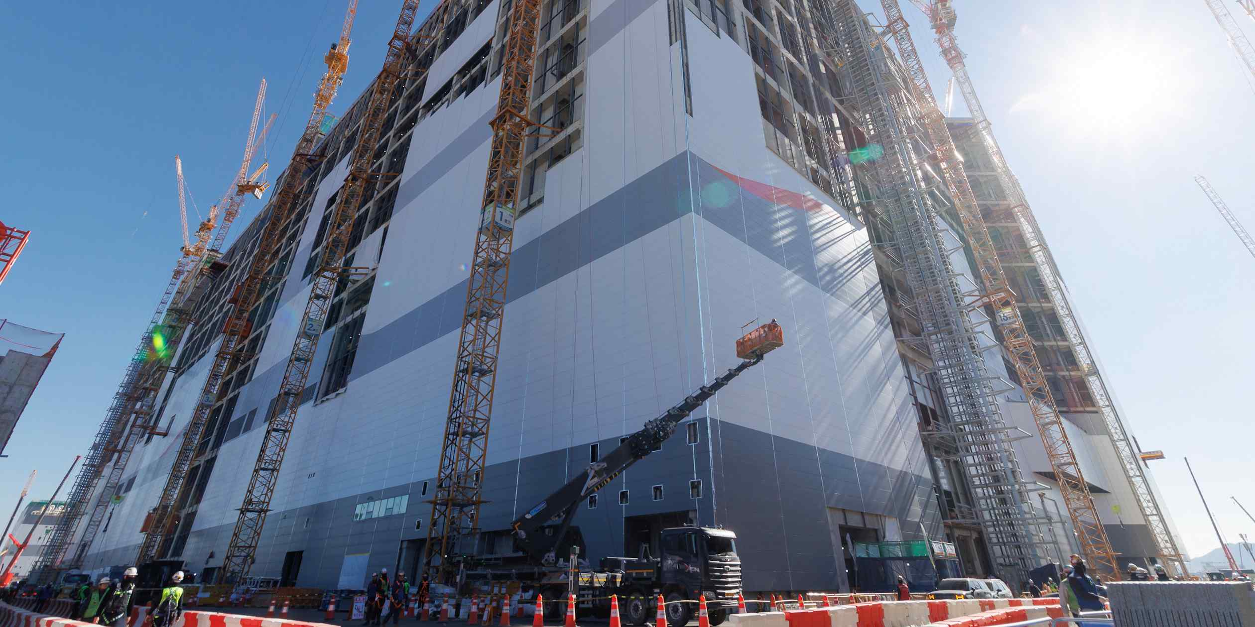
韩国用仁 —— 或许全球最高的半导体晶圆厂正拔地而起,坐落于韩国用仁的乡间丘陵之中,距首尔车程约 90 分钟。韩国存储芯片制造商 SK 海力士正在此建设其最大制造基地,以求跟上人工智能算力不断攀升的需求。
YONGIN, South Korea -- Perhaps the world's tallest semiconductor fabrication plant is rising among the rural hills of Yongin, a 90-minute drive from Seoul, as South Korean memory chipmaker SK Hynix builds its largest manufacturing complex to try to keep pace with demand for artificial intelligence computing.
本月一次媒体参访活动中,可以看到卡车在庞大的建设工地上穿梭忙碰,数千名工人争分夺秒抢建该晶圆厂,目标是于明年 2 月投入运营。
Trucks could be seen scurrying around the massive construction site on a press tour this month, as thousands of workers raced to build the fab, intended to be operational from February next year.
“为赶上目标日期,工地 24 小时不间断施工。你们正站在见证这段国家历史诞生的中心地带,”一位公司发言人表示。“即使在几年前亏损时期,我们也从未吝啬投资。” 随着超大规模数据中心通过长期协议加大对该公司动态随机存取存储器(DRAM)和高带宽存储器(HBM)芯片的订单,SK 海力xis 计划到 2034 年将其晶圆产能提高两倍(即变为三倍)。该公司还是英伟达 AI 加速器的关键 HBM 供应商。
"The site is under construction 24 hours a day to keep the [target] date. You are at the center of where this country's history is in the making," said a company spokesperson. "We have not spared investment, even when we suffered losses years ago." SK Hynix plans to triple its wafer capacity by 2034 as hyperscalers increase orders for the company's DRAM and high-bandwidth memory (HBM) chips through long-term agreements. The company is also a key HBM supplier for Nvidia's AI accelerators.
SK 海力士与这家领先 AI 芯片制造商的紧密合作提升了其全球声誉,推动其盈利和股价在过去几年大幅攀升。然而,英伟达首席执行官黄仁勋上周辞职构成潜在风险,因为 SK 海力士约 13% 的营收依赖英伟达。SK 集团会长崔泰源与黄仁勋建立了深厚私人交情。两人最近曾在韩国一家烧烤餐厅、台湾一场科技展以及美国一场颁奖典礼上会面。
SK Hynix's close partnership with the leading AI chipmaker has boosted its global reputation, driving earnings and its stock price sharply higher over the past few years. However, Nvidia CEO Jensen Huang's resignation last week poses a potential risk, as SK Hynix relies on Nvidia for about 13% of its revenue. Chey Tae-won, chairman of the SK Group conglomerate, had built a strong personal relationship with Huang. They recently met at a barbecue restaurant in South Korea, a tech exhibition in Taiwan and an awards ceremony in the U.S.
SK 海力士的用仁基地占地超 400 万平方米,该综合体将成为公司先进存储芯片生产的核心。(SK 海力士供图) 集团旗下建筑单位 SK Ecoplant 负责用仁项目施工,SK 海力士将在四座晶圆厂集群投资 600 万亿韩元(约合 4500 亿美元),其中包括斥资数十亿美元向荷兰供应商 ASML 采购先进极紫外光刻设备。
SK Hynix's Yongin site spans more than 4 million square meters, with the complex becoming the center of the company's advanced memory chip production. (SK Hynix) SK Ecoplant, a group construction unit, is working on the Yongin project, where SK Hynix is investing 600 trillion won ($450 billion) in the four-fab cluster, including spending billions of dollars on advanced extreme ultraviolet (EUV) chip manufacturing equipment from Dutch supplier ASML.
“能在一个迄今为止很可能是世界最高的[半导体]大楼、也是最大的晶圆厂工地上工作,我感到自豪,”工地负责人韩东勋(Han Dong-hoon)说。他指的是计划高度约为150米的首座晶圆厂Y1,相当于一栋50层的公寓楼。
"I am working with a sense of pride at a site that is, to date, likely the world's tallest [semiconductor] building and the largest fab," said Han Dong-hoon, construction site chief, referring to the first fab, Y1, planned at about 150 meters in height, equivalent to a 50-story apartment building.
韩东勋表示,约有2万人直接参与晶圆厂建设,包括后勤人员在内总共约2.5万人参与其中。
Han said about 20,000 people were working directly on building the fabs, with about 25,000 involved in total, including support staff.
他说:“我们至今未发生任何重大事故,正努力保持这一纪录,以期在2月底前完工。”
"We have yet to experience any major accidents, and we are striving to maintain this record as we work toward completion by the end of February," he said.
在Y1内部,一座名为“Trinity”(三位一体)的测试平台设施,得名于SK海力士、韩国政府和龙仁市政府的三方支持,将让本地中小企业测试自有技术,帮助它们缩短认证时间。
Inside Y1, a Trinity testbed facility, named after the trilateral backing of SK Hynix, the South Korean government and the Yongin city government, will let local small and medium-size enterprises test their own technologies, helping them reduce qualification times.
“评估期通常需要约六个月,长则长达两年,”SK海力士特种气体供应商TEMC首席执行官柳元阳(Yoo Won-yang)说。“但我们预计,如果Trinity晶圆厂建成,将大幅加快这一进程。”SK海力士的竞争对手三星电子也在该地区建厂。三星计划投资360万亿韩元建设六座晶圆厂,政府将该区域指定为国家产业园区,并承诺提供芯片生产所需的电力和水资源。
"The evaluation period typically takes about six months, or as long as two years," said Yoo Won-yang, CEO at TEMC, a special gas supplier to SK Hynix. "But we anticipate that if the Trinity fab is established, it will significantly accelerate that timeline." SK Hynix's rival Samsung Electronics is also building in the region. It plans to invest 360 trillion won in six fabs, with the government designating the area a national industrial complex and promising the power and water essential for chip production.
据今年早些时候视察工地的执政党共同民主党议员韩俊浩(Han Jun-ho)称,三星的建设进度落后于SK,截至3月仅获得了所需土地的约35%。三星拒绝就进度置评。
Samsung's construction timeline lags SK's, with only about 35% of the land needed acquired as of March, according to lawmaker Han Jun-ho of the governing Democratic Party, who visited the site earlier this year. Samsung declined to comment on progress.
除了龙仁集群外,SK海力士和三星还计划在西南部城市光州各建设两座晶圆厂,这是李在明总统政府在半导体、AI数据中心和实体AI三大领域推出的三大超级项目的一部分。SK集团会长崔泰源近期访问了该市,以展示对该项目的承诺,此前一些在野党政客质疑其商业可行性,称该项目是政府“出于政治动机”推动的。
As well as the Yongin cluster, SK Hynix and Samsung are planning two fabs each in the southwestern city of Gwangju as part of President Lee Jae Myung government's three megaprojects for semiconductors, AI data centers and physical AI. SK Chairman Chey recently visited the city to show his commitment to the project, as some opposition party politicians questioned its commercial viability, saying it was "politically motivated" by the government.